rohitshubham
Ambassador of Buzz
so, nvidia released their new GK 208 architecture few months back to power their low-mid range GPU's.
now i did a bit of googling and decided to post a review about it from the info.(sorry for bad english.... the material is translated from japanese)
*www.thinkdigit.com/forum/attachments/reviews/11382d1374140515-nvidias-gk-208-architecture-xo4l.jpg
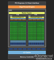
Block Diagram:-
*www.thinkdigit.com/forum/attachments/reviews/11383d1374140515-nvidias-gk-208-architecture-021.jpg
First of all, I think I want to make sure of that GK208 is whether the GPU core what, basically, and 640 DDR3 GT, which is a high-end model " Georce GTX 650 -based employed by "and" GK107 "core The nice understanding that those while, and it has a 64bit half the width of the specification of the memory controller. In the case of the first-generation Kepler architecture adopted GPU, including the GK107 core, shader processor "CUDA Core" 192 group, set and texture unit of 16 based and L1 cache, and geometry engine of one group called "PolyMorph Engine 2.0" Become a, Configuring barrel operation unit "Streaming Multiprocessor eXtreme" (below, SMX) a.To configure "Graphics Processing Cluster" (below, GPC) the Conclusion 2 based on the SMX, was to be "mini GPU" in conjunction with the rasterizer. And if the GK107, the number of GPC This is a one-group, the number of SMX is two, CUDA Core number is a translation a 384 basis but, GK208 alone are the same around here. Based on the block diagram of the GK107 core, was shown to the right, it's block diagram of the GK208 you guess 4Gamer but, in fact, one based on the ROP partition collectively and 64bit memory controller, the ROP unit of eight The cut from the block diagram of the GK107, to be or had just trimmed the arrangement. In the GPU only sharpened the 64bit memory controller from GK107, why NVIDIA is what gave the model number that rather than GK208 "GK108". Us will be inferred from here, the potential in the CUDA around high reason. If you let me be the talk of the CUDA GPU and a little, Tesla architecture since corresponding to CUDA, NVIDIA is "to GPU Compute Capability has given a value of ". Compute Capability to be expressed in the form of "XX" The developer page of NVIDIA 's can see in, but what the numbers mean I as follows. It is not is to know "what to be let as a CUDA processor" and "generation of the GPU core" and see this Compute Capability.
Before the decimal point : major revision. Which is defined by the core architecture. 3 If it is 2, Kepler if 1, Fermi if Tesla
And from here's the important, Compute Capability of GK208 is 3.5s. In the NVIDIA GPU made in June 2013, this is the highest value. "GK110 only been achieved Compute Capability 3.5 With the exception of the GK208" It may be easier to understand is better explained, "but, at any rate, if you are just Compute Capability," GK208, theGeForce GTX 680 and, "" GeForce GTX 770 "- -GK104 these to adopt the core is 3.0 - is of the above. so, it's computation capabilities are very high, much higher than GK107. I think in that sense, appears to be good but "GK118" model number, but it is a core that does not correspond to the GK208 "GK108" at least and understand. Honestly, why NVIDIA has developed all the way to the low-end market and entry, the "new GPU core with a set of Compute Capability same as GK110" does not say anything. So from that share the basic design and notebook PC is GPU of this class, " OEM major enough to affect the GPU shipment planning of NVIDIA from, been requested to GPU with full support for CUDA of the latest generation, to respond to it seems to be whether it is line realistic is that "has been introduced also to the desktop market in passing, but the possibility of whether that so actually, NVIDIA is willing to explain because close to zero as possible. It's going to be, "Oh, I see" and such Notebook PC If you find the one, and that "Oh, I made the GK208 Good luck, but I wish it was last lost to OEM winning battle with Intel" and if you do not come out or would not than be.
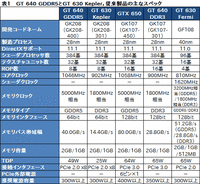
While still having the light of the above, compared to 640 DDR3, GT 630 Fermi GT and GTX 650, the specs of 630 Kepler GT and 640 GDDR5 GT is Table 1 a.Connection interface of the GPU in a PCI Express 2.0, moreover 8 lane and I just for that eye-catching, but this, convincing if it 's Assuming the implementation of the notebook PC, aimed at the reduction of power consumption. (Thermal Design Power, thermal design power consumption) in the TDP, about 75% of the 640 DDR3 GT, is to contribute to 630 Kepler GT has be reduced to about 38% of the 630 Fermi GT, 640 GDDR5 GT is only memory interface It looks good look without, and there is also a reduction of PCI Express connection number of lanes.
Another, in the memory around, 640 GDDR5 GT will want to pay attention to the point where memory clock by a very high (= data rate), which extends the memory bus bandwidth 640 DDR3 ratio GT. On the other hand, is 630 Kepler GT, because the interface is reduced by half of the memory remains the same clock as the DDR3 version of the 630 Fermi GT, memory bus bandwidth has also become one-half.
The 630 Kepler GT, while more than texture units and the number of CUDA Core number, in the ROP number of units, the (DDR3 version) GT 630 Fermi, and always have been taken place in the memory bus bandwidth and the operating clock, it is in fact in order to check what kind of produce results in the test, it will be an important check items in the test stage, which will be described later.
another website's table/;
Now, we easily see that the TDP is very low and that's a very good advantage especially for mobile computing.
As Nvidia has just informed us it also support the new GeForce GT 640 and GeForce GT 630 DirectX 11.1 only with the feature level 11.0. So nothing changes compared to the rest of the Kepler cards regarding the Microsoft API. Why the information on the website fails differently to the rest of GeForce cards, remains a secret from Nvidia.
-------------------------------------------------------------------------------------------------------------------------------------------------------
now, i have seen people drooling over the new architecture and trying to get their hands on it. there are people who returned their laptop cause it shipped with older architecture.
Since i am not an expect but someone here said"Really kind of seems to me that they've been cutting the D2H & H2D bandwidth in a potential effort to save on power consumption"
So, the power/watt is very high of the GK208 architecture.
For more information go to:*devtalk.nvidia.com/default/topic/5...tops-cards-will-support-most-sm_35-features/1 (kindly read all the pages as there is really nice info after 2nd page)
and
¿·¥³¥¢¡ÖGK208¡×¤Ã¤Æ¤Ê¤ó¤À¡© ÆÍÇ¡Åо줷¤¿¿··¿¡ÖGeForce GT 640¡õ630¡×¤ò¥Æ¥¹¥È - 4Gamer.net (is in JApanese).so, many reviews have said that there are few advantages and disadvantages of this architecture.
there is decrease in raw performance but in increase in computational power and most importantly the performance/watt of power consumed will give very high battery life and lower TDP which will result in more effective cooling.where as developers claim it to be much more better architecture than the previous generations.
now i did a bit of googling and decided to post a review about it from the info.(sorry for bad english.... the material is translated from japanese)
*www.thinkdigit.com/forum/attachments/reviews/11382d1374140515-nvidias-gk-208-architecture-xo4l.jpg
Block Diagram:-
*www.thinkdigit.com/forum/attachments/reviews/11383d1374140515-nvidias-gk-208-architecture-021.jpg
First of all, I think I want to make sure of that GK208 is whether the GPU core what, basically, and 640 DDR3 GT, which is a high-end model " Georce GTX 650 -based employed by "and" GK107 "core The nice understanding that those while, and it has a 64bit half the width of the specification of the memory controller. In the case of the first-generation Kepler architecture adopted GPU, including the GK107 core, shader processor "CUDA Core" 192 group, set and texture unit of 16 based and L1 cache, and geometry engine of one group called "PolyMorph Engine 2.0" Become a, Configuring barrel operation unit "Streaming Multiprocessor eXtreme" (below, SMX) a.To configure "Graphics Processing Cluster" (below, GPC) the Conclusion 2 based on the SMX, was to be "mini GPU" in conjunction with the rasterizer. And if the GK107, the number of GPC This is a one-group, the number of SMX is two, CUDA Core number is a translation a 384 basis but, GK208 alone are the same around here. Based on the block diagram of the GK107 core, was shown to the right, it's block diagram of the GK208 you guess 4Gamer but, in fact, one based on the ROP partition collectively and 64bit memory controller, the ROP unit of eight The cut from the block diagram of the GK107, to be or had just trimmed the arrangement. In the GPU only sharpened the 64bit memory controller from GK107, why NVIDIA is what gave the model number that rather than GK208 "GK108". Us will be inferred from here, the potential in the CUDA around high reason. If you let me be the talk of the CUDA GPU and a little, Tesla architecture since corresponding to CUDA, NVIDIA is "to GPU Compute Capability has given a value of ". Compute Capability to be expressed in the form of "XX" The developer page of NVIDIA 's can see in, but what the numbers mean I as follows. It is not is to know "what to be let as a CUDA processor" and "generation of the GPU core" and see this Compute Capability.
Before the decimal point : major revision. Which is defined by the core architecture. 3 If it is 2, Kepler if 1, Fermi if Tesla
- After the decimal point : minor revision. I go up new feature is added.GK104 core condition which became the advance guard of the Kepler architecture 0, GK110 core that supports and "Dynamic Parallelism" and "Hyper-Q" is like 5
| *www.4gamer.net/games/160/G016083/20130628096/TN/026.jpg |
| *www.4gamer.net/games/160/G016083/20130628096/TN/027.jpg |
While still having the light of the above, compared to 640 DDR3, GT 630 Fermi GT and GTX 650, the specs of 630 Kepler GT and 640 GDDR5 GT is Table 1 a.Connection interface of the GPU in a PCI Express 2.0, moreover 8 lane and I just for that eye-catching, but this, convincing if it 's Assuming the implementation of the notebook PC, aimed at the reduction of power consumption. (Thermal Design Power, thermal design power consumption) in the TDP, about 75% of the 640 DDR3 GT, is to contribute to 630 Kepler GT has be reduced to about 38% of the 630 Fermi GT, 640 GDDR5 GT is only memory interface It looks good look without, and there is also a reduction of PCI Express connection number of lanes.
| *www.4gamer.net/games/160/G016083/20130628096/TN/030.gif |
| *www.4gamer.net/games/160/G016083/20130628096/TN/029.jpg |
The 630 Kepler GT, while more than texture units and the number of CUDA Core number, in the ROP number of units, the (DDR3 version) GT 630 Fermi, and always have been taken place in the memory bus bandwidth and the operating clock, it is in fact in order to check what kind of produce results in the test, it will be an important check items in the test stage, which will be described later.
another website's table/;
| Nvidia GeForce GT640 (DDR3) | Nvidia GeForce GT640 (GDDR5) | Nvidia GeForce GT630 (Fermi) | Nvidia GeForce GT630 (Kepler) | |
|---|---|---|---|---|
| GPU | GK107 | GK208 | GF108 | GK208 |
| The area | 118 mm2 | ~ 90 mm2 | 116 mm2 | ~ 90 mm2 |
| DirectX Level | 11.0 | 11.1 | 11.0 | 11.1 |
| GPU-based clock | 900 MHz | 1,046 MHz | 810 MHz | 902 MHz |
| Shader units | 384 | 384 | 96 | 384 |
| ROPs | 16 | 8 | 4 | 8 |
| TMUs | 32 | 32 | 16 | 32 |
| Amount of memory | 2,048 MB DDR3 | 1,024 MB GDDR5 | 1,024 MB DDR3/GDDR5 | 2,048 MB DDR3 |
| Memory Bandwidth | 28.5 GB / s | 40.0 GB / s | 28.8 / 51.2 GB / s | 14.4 GB / s |
| Memory interface | 128 bit | 64 bit | 128 bit | 64 bit |
| TDP | 65 W | 49 W | 65 W | 25 W |
As Nvidia has just informed us it also support the new GeForce GT 640 and GeForce GT 630 DirectX 11.1 only with the feature level 11.0. So nothing changes compared to the rest of the Kepler cards regarding the Microsoft API. Why the information on the website fails differently to the rest of GeForce cards, remains a secret from Nvidia.
-------------------------------------------------------------------------------------------------------------------------------------------------------
now, i have seen people drooling over the new architecture and trying to get their hands on it. there are people who returned their laptop cause it shipped with older architecture.
Since i am not an expect but someone here said"Really kind of seems to me that they've been cutting the D2H & H2D bandwidth in a potential effort to save on power consumption"
So, the power/watt is very high of the GK208 architecture.
For more information go to:*devtalk.nvidia.com/default/topic/5...tops-cards-will-support-most-sm_35-features/1 (kindly read all the pages as there is really nice info after 2nd page)
and
¿·¥³¥¢¡ÖGK208¡×¤Ã¤Æ¤Ê¤ó¤À¡© ÆÍÇ¡Åо줷¤¿¿··¿¡ÖGeForce GT 640¡õ630¡×¤ò¥Æ¥¹¥È - 4Gamer.net (is in JApanese).so, many reviews have said that there are few advantages and disadvantages of this architecture.
there is decrease in raw performance but in increase in computational power and most importantly the performance/watt of power consumed will give very high battery life and lower TDP which will result in more effective cooling.where as developers claim it to be much more better architecture than the previous generations.
Attachments
Last edited: